Computational subwavelength optics

Introduction
Subwavelength diffraction optical element with binary features that are artificially structured on a suitable optical substrate, such as the one shown in Fig. I below, can imitate a phase-varying refractive surface and mimic the effect of, e.g. thin-film coating, supplying antireflection, form birefrsingence, polarizing, or filtering effects, etc.
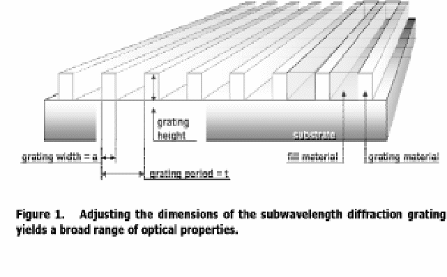
We speak of ‘binary optics’ when considering the interactions of light with such kind of binary features presented by a diffractive optical element. ‘Subwavelength’ is referred to the physical condition for which the wavelengths of the interacting light in the problem considered are many times larger than the sizes of the binary features of the diffractive optical element. The problem of interactions of subwavelength diffractive optical element with light in the visible or larger wavelength region can be considered as a subfield of nano-optics, one of the hottest research fields in the frontier of applied physics and technology.
To give an idea of the feature size of the said diffractive optical elements, wafer-based substrates having binary feature less than 60 nm wide have been recently fabricated (around year 2003) in a commercial scale thanks to the breakthrough in nanotechnology. [1, 2]. The breakthrough in the commercial fabrication of such wafer-based optical chips promises immense applications in optical and optoelectronics system design. The key reason to the immense potentiality of an nano-optical subwavelength optical element lies in its revolutionarily tiny dimension, robust performance, and versatility that is readily integrated with existing wafer-based optoelectronics “on a chip”, which physical size can be customized for architectural requirement.
Conventionally, geometrical optics is the working principle to lens system design which often constitutes an indispensable component in an optoelectronics or telecommunication system. In practice, fabrication of geometrical lenses is constrained by many limitations in precision technology. On the other hand, subwavelength binary optical elements (which can be fabricated on a large scale on silicon-based wafer thanks to the advent of the newly available nano-optics technology as mentioned above) is possessed of an edge over the conventional fabrication of optical systems. One could liken the difference between the two approaches of optical design in terms of analogue versus digital electronic systems design. For example, by employing the subwavelength binary optics approach, one could in principle theoretically design a 96-m diameter optical element that is capable of focusing a 10-m infrared radiation on to a 100-m focal plane [3] without worrying much about the constraints from the actual fabrication difficulties. The essential ingredient that makes things work here is the specific binary nano pattern (the “digital electronics” analogue) rather than the overall geometry of the diffractive lenses (the “analogue electronics” analogue).
Referring to the above example, if such delicate optical output is to be achieved based on the conventional geometrical optics approach (e.g. via a concave lens), the required geometry and precision of the fabrication of such lenses could be technically difficult to cater for, or even impossible. Quite generally, traditional optical materials require a relatively large size and delicate precision technique to create the same optical effect.
For example, traditional optics (i.e. geometrical optics) would find it too demanding (e.g. in terms of high cost and precision technology) to fabricate an optical component of very tiny size, say, 1 mm. This is a ‘hardware’ problem (in contrast to the ‘software’ problem, as shall be explained in the following paragraph) subjected to severe technological and physical limitations.
As a comparison, the functionalities of subwavelenght optics are driven by ‘software’ design (the binary nano features) rather than by the precise fabrication of conventional optical lenses (the ‘hardware’). In binary optics, one’s task is to design an appropriate binary profile on the diffractive optical element that would produce desired optical responses by making use of numerical computations running on a high performance computer or a workstation. In other words, this is a programming design that simulates the actual optical system. As mentioned, the physical fabrication (the hardware aspect) of the binary nano profile (say, at a physical size of as tiny as 60 nm) can be left to the nanotechnology companies.
Technically speaking, the real difficulty to design nano optics profile for a given optical output is basically due to overwhelmingly tiny feature of the optical diffractive element. Generically, the feature size of the binary profile on the optical chip is much smaller than the wavelengths of, say, visible or infrared light. In this subwavelength domain, the interactions between light and the subwavelength optical elements could no more be sufficiently described by mere conventional optics phenomena such as diffraction, reflection or refraction. In the subwavelength domain, the dimension of the binary structure is sufficiently small that no diffracted orders propagate, but at the same time also it is not possible to apply the simple approximations of homogeneous medium [4]. In effect, scalar diffraction theory [5], of which the working basis of Fourier and Fraunhofer optics is based upon, is no longer valid. Such scenario renders difficulty to predict the optical responses as a function of a given general binary nano profile on a general basis. This is to be contrasted with the conventional Fraunhofer optics which allows us to predict the optical responses with relative ease via theoretical approximations or with the aid of available software such as the ZEMEX or ASAP (which implicitly assume the validity of scalar diffraction theory in their built-in codes).
On the ground of the fundamental physics principles that governs the behaviour of light and their interactions with matter at the classical scale, scalar diffraction theory for optical phenomena is merely an approximation form of the more general Maxwell theory. Hence, to predict the precise optical response of a general binary diffractive optical element in the subwavelength domain, one has to go back to the full Maxwell equations, solving them in a rigorous manner by numerical electromagnetic methods. This is a computationally demanding task.
In short, this is essentially a research field in the domain of a less conventional type of diffractive optics, which prime concern is to reshape the input wavefront into desired optical responses by making use of the artificial subwavelength patterns (generally in the form of binary features) on the surface of these diffractive optical elements. Numerical solutions to the full Maxwell equations are to be simulated on a high performance computer for such purpose. Here lies the challenge which this research proposal is attempting to undertake.
Objectives
The prime objective of this research project is to build a numerical machinery on the workstation/high performance computer that can simulate the subwavelength optical response from a diffractive optical element with nano features. This numerical machinery, if successfully developed, shall become a very powerful tool that allows one to design the nano feature on the diffractive optical element that could provide desired optical responses for a wide range of optoelectronic applications. For example, with the numerical machinery, one can design binary nano features on an optical chip that can mimic the functionalities of, e.g. polarizer, beam splitter, optical valve, optical switching device, optical filter/combiners, photodetector, photonic bandgap device, etc.
The second objective of this research project, subjected to the outcome of the first objective mentioned above, is aiming at the actual realization of some mm size optical chips that could be integrated into some optoelectronic components to provide noble functionalities. More specifically, I am thinking of the possibility of integrating the subwavelenght optical element into a LED wafer during their manufacturing procedure. The intended product is a LED that would emit polarized light (rather than ordinary non-polarised light). Of course, there is a whole list of non-exhaustive possibilities on the applications of such kind of novel optical chips in telecommunication and optoelectronics. The polarized LED is merely one illustrative example of those.
The third objective, which is not as “physical” in terms of the actual research findings, is to initiate an opportunity for the researcher involved (e.g. me and my potential students) to acquire the very valuable and pragmatic skill of building up a ‘numerical apparatus’ to “experiment” (via computer simulation) on real physical systems. This is essentially a computational intensive training, of which the technical skill derived could also be applied to other fields of research, such as the simulation of interactions of a many-body system, simulation of interactions (both linear as well as non-linear ones) of light through a medium of special interest such as liquid crystals, or numerically solving some highly non-trivial non-linear dynamical systems.
Methodology
The modeling of the optical responses of a subwavelength optical element is to be implemented on a workstation by resorting to numerical methods that are commonly used in computational electrodynamics, e.g. finite-difference time-domain method (FDTD) [6]. Computer codes are to be developed to numerically simulate the propagation of the light waves throughout their course of interactions with the subwavelength diffractive optical element. This is achieved by numerically solving the 3-D Maxwell equations that describe the propagation of light which is diffracted by the non-trivial binary structure of the diffractive optical elements. An optimization procedure will also be developed to perform a looped feedback to the designed profile to optimize the desired optical responses.
A flowchart representing the flow of the computational procedure is given in Fig. II.
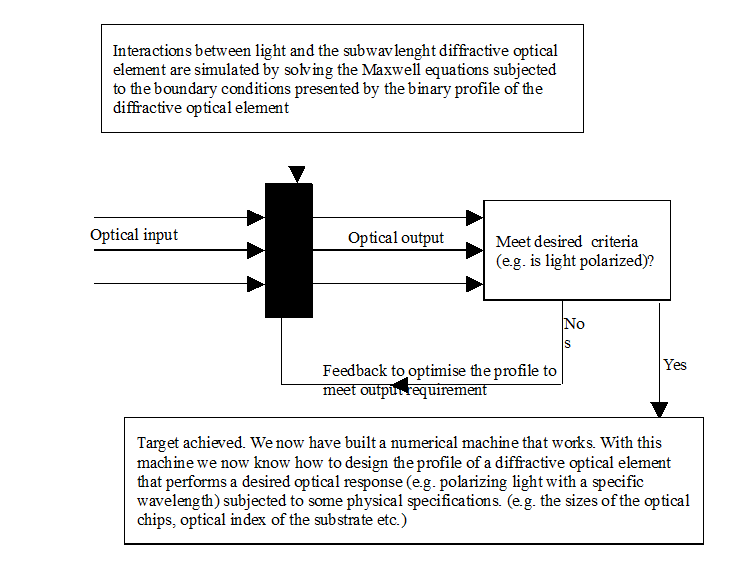
Fig. 2: Flowchart of optimisation of the profile and simulation of interactions between light and the diffractive optical element
The computational algorithms for such purpose are well documented and is readily available [6,7,8,9]. Mathematica and Fortran programming shall be employed for the purpose of developing my own codes. Due to the computationally intensive nature of the research project, high performance workstation/computer is a must.
Outcome
1. A numerical machinery in the form of programming codes sitting inside the hard disk of the workstation shall be developed. Such codes shall be the main ‘physical’ outcome of the research project.
2. The eventual realisation of this numerical machinery would also mean the KNOWLEDGE to design subwavelength diffractive optical elements shall be acquired. With this knowledge, we would be able to, for example, design a nano scale binary profile on an optical chip of 1 mm in size that could polarise light of a particular wavelength that passes through the optical chip.
3. Very handy computational skill using high performance workstation shall be learnt and acquired. Such highly non-trivial skill shall be a very valuable asset to the involved researchers (particularly to Malaysian researchers) for many potential applications in other fields in the future.
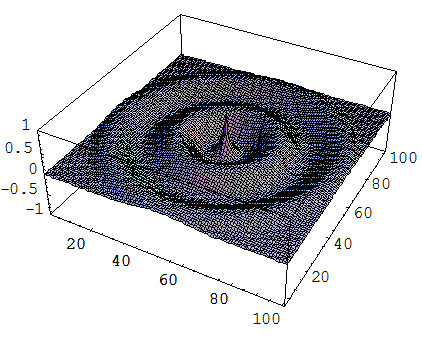
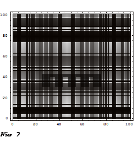
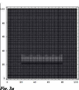
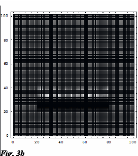
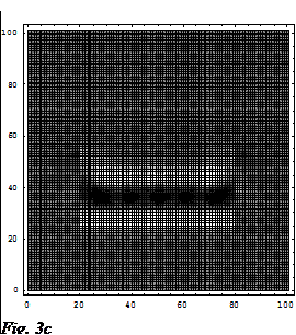
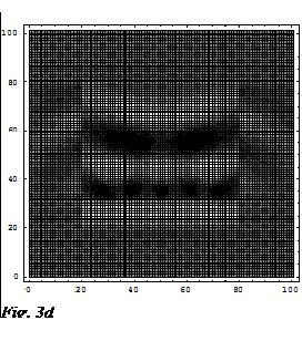
As an example of part of the result from this research topic, I illustrate here the diffraction pattern of the electromagnetic field propagating through a SWDOE (graphic generated by Chan Tang Yong, then a final year project student under my supervision). Fig. 2 illustrate a binary SWDOE's reflective index profile, which dimension is a few time the size of the EM wavelength in the simulation. Fig.3a - Fig.3d show the optical outcome after the incident EM wave (coming from the bottom) interacts with the SWDOE.
The Importance And The Benefits Of The Research
The importance of the research in subwavelength optical elements lies in their immense potential applications in optoelectronics and telecommunication systems.
The advantages of subwavelength optical element are many.
1. Subwavelength diffractive optical elements can be fabricated in the form of wafer-based optical chips that are readily integrated with silicon-based electronic components. Due to its compact size as well as its versatility to effectively imitate many optical functionalities via the artificial binary pattern, subwavelength optics possesses very strong advantages against conventional optical systems, especially if the problem of integration of optical functionalities into existing optoelectronics systems is a major concern. In essence, subwavelength diffractive optical elements supply many superior architectural benefits for more compact optical component designs in optoelectronics systems.
2. In addition, generically, subwavelength optical elements provide higher efficiency in optical signal processing when compared with conventional optical systems [10].
The benefits and advantages to acquire the know-how of designing subwavelength binary optical chips are obvious. Subwavelength binary optics opens up a whole new direction of applications in applied optics, optoelectronics and communication systems because binary optical chips could be easily integrated into existing optoelectronics systems for more compact and versatile optical functions. But above all, from a pragmatist point of view, the most important benefit of this research project is that: it is reasonably “doable” in the context of Malaysian research ambient. “Doable” here means it doest not require a lot of money to buy machines for experimentation purpose (as this is only a simulation on a computer). At the same time, the technicalities to perform the computational simulation are also not known to pose much serious difficulties of fundamental nature except being messy and cumbersome. The latter can be overcome by perseverance, enthusiasm and determination.
In short, the know-how to perform such simulations and design is of utmost necessary if we wish to produce optical chips of such high applicability in the near future in Malaysia.
This is a nanotechnology-related research topic that perfectly suits the Malaysian context: affordable, doable (in terms of intellectual and research capabilities), significant (possessed of immense potential of applications). The ultimate commercial Malaysian production of nano-optical chips must first leap from here: the know-how to simulate the subwavelength diffractive optical element.
References
[1] See http://www.nanoopto.com/ for the company that has come up with the breakthrough technology to mass produce nano-optical chips.
[2] Hubert Kostal, Nano-optics White Paper #001, downloadable from http://www.nanoopto.com/technology/index.html.
[3] D. W. Prather and J.N. Mait, J. Opt. Soc. Am. A15, 1599 (1998).
[4] Philippe Lalanne and Mike Hutley, in Encyclopedia of optical engineering (Dekker, New York)
[5] Max Born and Emile Wolf, Principles pf Optics, 3rd ed. (Pergamon Press, New York, 1965).
[6] Allen Taflove, Computational electrodynamics: The finite-difference time-domain method, 2nd ed. (Artech House, Norwood).
[7] Many outstanding works on the numerical computation of binary subwavelength diffractive-lens design using FDTD method have been done by the group of Dennis W. Prather. See his personal webpage at: http://www.eecis.udel.edu/~dprather/.
[8] Some papers on subwavelength diffractive optical element that are immediately relevant to the this research proposal, particularly those done by the group in ref. [5] are: J. N. Mait, D. W. Prahter and M. S. Mirotznik, Opt. Lett. 23, 1343 (1998); D. W. Prather and S. Shi, J. Opt. Soc. Am. A16, 1131 (1998); ibid., Opt. Eng. 39. 1850 (2000); M. S. Mirotznik et al., App. Opt. 39, 2871 (2000); S. Shi et al., Opt. Eng. 40, 503 (2001).
[9] Some useful FDTD numerical packages has been developed in other related field such as printed circuit board (PCB) modeling. See the personal webpage by DR. Fabian Kung at http://pesona.mmu.edu.my/~wlkung/.
[10] Michael W. Farn, App. Opt. 22, 4453 (1992).